Showing posts with label Basic Electronics. Show all posts

Thursday 20 April 2017

Branches of electronics

Electronics has branches as follows:

  1. Digital electronics
  2. Analog electronics
  3. Microelectronics
  4. Circuit design
  5. Integrated circuits
  6. Optoelectronics
  7. Semiconductor devices
  8. Embedded systems


Digital electronics:-We know there are two types of signals, one is analog or continuous signal and the second one is Digital or discrete signal. So the science or field of research in the area of engineering is termed as Analog and Digital Electronics respectively. Now coming to the area of Digital Electronics, it is essential to understand wide range of applications from industrial electronics to the fields of communication, from micro embedded systems to military equipment. The main and perhaps the most revolutionary advantage of digital electronics is the decrease in size and the improvement in technology.
      we have enlightened the very important field of Digital Electronics i.e. Binary Arithmetic and Boolean algebra. And we have discussed about them in elaborated manner. From binary additionbinary subtractionbinary multiplication and binary division to the basics of Boolean algebra. After that we have written topics about various types of codes such as ASCII codeGray CodeHamming code which have made the input output format very easy. Then various types of logic gates (AND gateOR gateNOT gateNAND gateNOR gateEX-OR gate) have been discussed in an elaborated manner with diagrams, explanations and truth tables to make each one of them very easy to understand.
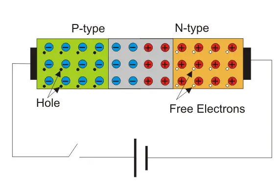
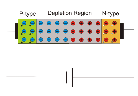
Monday 17 April 2017

Series & Parallel Resistors

Resistors in Series:-

Resistors are said to be connected in series when they are daisy chained together in a single line resulting in a common current flowing through them.

                       A series circuit is a circuit in which resistors are arranged in a chain, so the current has only one path to take. The current is the same through each resistor.


Image result for resistor series connection


                     Rtotal = R1 + R2 +R3 +............................


Resistors in Parallel:-

                  A parallel circuit is a circuit in which the resistors are arranged with their heads connected together, and their tails connected together. The current in a parallel circuit breaks up, with some flowing along each parallel branch and re-combining when the branches meet again. The voltage across each resistor in parallel is the same.

resistors_in_series_10


Resistor color Coding

RESISTOR COLOR CODING:-
                  The electronic color code is used to indicate the values or ratings of electronic components, usually for resistors.

A diagram of a resistor, with four color bands A, B, C, D from left to right A diagram of a 2.7 MΩ color-coded resistor.
To distinguish left from right there is a gap between the C and D bands.
  • band A is the first significant figure of component value (left side)
  • band B is the second significant figure (some precision resistors have a third significant figure, and thus five bands).
  • band C is the decimal multiplier
  • band D if present, indicates tolerance of value in percent (no band means 20%)

For example:-
       A resistor with bands of Yellow, Violet ,red and Gold has first digit 4 (yellow in table below), second digit 7 (violet), followed by 2 (red) zeros: 4,700 ohms. Gold signifies that the tolerance is ±5%, so the real resistance could lie anywhere between 4,465 and 4,935 ohms.


Sunday 16 April 2017

Capacitor

CAPACITOR:-
                         Capacitor is a passive element that stores electric charge statistically and temporarily as an static electric field. It is composed of two parallel conducting plates separated by non-conducting region that is called dielectric, such as vacuum, ceramic, air, aluminum, etc. The capacitance formula of the capacitor is represented by,
 C is the capacitance that is proportional to the area of the two conducting plates (A) and proportional with the permittivity ε of the dielectric medium. The capacitance decreases with the distance between plates (d). We get the greatest capacitance with a large area of plates separated by a small distance and located in a high permittivity material. The standard unit of capacitance is Farad, most commonly it can be found in micro-farads, pico-farads and nano-farads. 
  
Image result for CAPACITOR

Types of Capacitors

The various types of capacitors have been developed to overcome these problems in a number of ways.

Paper Capacitor

It is one of the simple forms of capacitors. Here, a waxed paper is sandwiched between two aluminium foils. Process of making this capacitor is quite simple. Take place of aluminium foil. Cover this foil with a waxed paper. Now, cover this waxed paper with another aluminium foil. Then roll up this whole thing as a cylinder. Put two metal caps at both ends of roll. This whole assembly is then encapsulated in a case. By rolling up, we make quite a large cross-sectional area of capacitor assembled in a reasonably smaller space.paper capacitor

Air Capacitor

There are two sets of parallel plates. One set of plates is fixed and another set of plates is movable. When the knob connected with the capacitor is rotated, the movable set of plates rotates and overlapping area as between fixed and movable plates vary. This causes variation in effective cross-sectional areas of the capacitor. Consequently, the capacitance varies when one rotates the knob attached to the air capacitor. This type of capacitor is generally used to tune the bandwidth of a radio receiver.variable air capacitor

Plastic Capacitor

When various plastic materials are used as dielectric material, the capacitors are said to be plastic capacitors. The plastic material may be of polyester, polystyrene, polycarbonate or poly propylene. Each of these materials has slightly different electrical characteristics, which can be used to advantage, depending upon the proposed application.
This type of capacitors is constructional, more or less same as paper capacitor. That means, a thin sheet one of the earlier mentioned plastic dielectrics, is kept between two aluminium foils. That means, here the flexible thin plastic sheet is used as dielectric instead of waxed paper. Here, the plastic sheet covered by aluminium foil from two sides, is first rolled up, then fitted with metal end caps, and then the whole assembly is encapsulated in a case.

Plastic Film Capacitor

Plastic capacitor can be made also in form of film capacitor. Here, thin strips or films of plastic are kept inside metallic strips. Each metallic strip is connected to side metallic contact layer alternatively; as shown in the figure below. That means, if one metallic strip is connected to left side contact layer, then the very next is connected to right side contact layer. And there are plastic films in between these metallic strips. The terminals of this type of capacitors are also connected to side contact layer and whole assembly is covered with insulated non metallic cover as shown.plastic capacitor

Silvered Mica Capacitor

A silvered mica capacitor is very accurate and reliable capacitor. This type of capacitors has very low tolerance. But on the other hand, cost of this capacitor is quite higher compared to other available capacitors in the market. But this high cost capacitor can easily be compensated by its high quality and performance. A small ceramic disc or cylinder is coated by silver compound. Here, electrical terminal is affixed on the silver coating and the whole assembly is encapsulated in a casing.

Ceramic Capacitor

Construction of ceramic capacitor is quite simple. Here, one thin ceramic disc is placed between two metal discs and terminals are soldered to the metal discs. Whole assembly is coated with insulated protection coating as shown in the figure below.Ceramic Capacitor

Principle of Capacitor

As a capacitor is passive component, it does not generate energy. But it is able to store energy from an energy source like a battery or another charged capacitor. When a battery (DC Source) is connected across a capacitor, one surface, named plate I gets positive end of the battery and another surface, named plate II gets negative end of the battery. When battery is connected, the full voltage of that battery is applied across that capacitor. At that situation, plate I is in positive potency with respect to the plate II. Current from the battery tries to flow through this capacitor from its positive plate (plate I) to negative plate (plate II) but cannot flow at max value due to separation of these plates with an insulating material. Rather a very small current will flow through this insulating material (dielectric) from Positive to Negative plate depending upon the value of strength of this dielectric.
An electric field will form inside the capacitor dielectric from positive to negative plate. As time goes on, positive plate (plate I) will accumulate positive charge from the battery and negative plate (plate II) will accumulate negative charge from negative end of the battery. After a certain time, the capacitor holds maximum amount of charge as per its capacitance with respect to this voltage. This time span is called charging time of this capacitor.charging capacitorNow, after removing this battery from this capacitor, these two plates will hold positive and negative charges with respect to a certain voltage level for long time. Thus this capacitor acts as energy source.charged capacitorIf two ends (plate I and plate II) get shorted through a load, a current will flow through this load from plate I to plate II up to all charges get vanished from both plates. This time span is known as discharging time of the capacitor.

discharged capacitor

Energy Stored in Capacitor


While capacitor is connected across a battery, charges come from the battery and get stored in the capacitor plates. But this process of energy storing is step by step only.At the very beginning, capacitor does not have any charge or potential. i.e. V = 0 volts and q = 0 C.energy stored in capacitorNow at the time of switching, full battery voltage will fall across the capacitor. A positive charge (q) will come to the positive plate of the capacitor, but there is no work done for this first charge (q) to come to the positive plate of the capacitor from the battery. It is because of the capacitor does not have own voltage across its plates, rather the initial voltage is due to the battery.

First charge grows little amount of voltage across the capacitor plates, and then second positive charge will come to the positive plate of the capacitor, but gets repealed by the first charge. As the battery voltage is more than the capacitor voltage then this second charge will be stored in the positive plate. At that condition a little amount of work is to be done to store second charge in the capacitor. Again for the third charge, same phenomenon will appear. Gradually charges will come to be stored in the capacitor against pre-stored charges and their little amount of work done grows up.energy stored in capacitorIt can’t be said that the capacitor voltage is fixed. It is because of the capacitor voltage is not fixed from the very beginning. It will be at its maximum limit when potency of capacitor will be equal to that of the battery. As storage of charges increases, the voltage of the capacitor increases and also energy of the capacitor increases. So at that point of discussion the energy equation for the capacitor can’t be written as energy (E) = V.q As the voltage increases the electric field (E) inside the capacitor dielectric increases gradually but in opposite direction i.e. from positive plate to negative plate.Here dx is the distance between two plates of the capacitor.energy stored in capacitorCharge will flow from battery to the capacitor plate until the capacitor gains as same potency as the battery. So, we have to calculate the energy of the capacitor from the very begging to the last moment of charge getting full.

Resistors

resistor offers resistance to the flow of current. The resistance is the measure of opposition to the flow of current in a resistor. More resistance means more opposition to current. The unit of resistance is ohm and it is represented as Ω. When one volt potential difference is applied across a resistor and for that one ampere of current flows through it, the resistance of the resistor is said to be one Ω. Resistor is one of the most essential passive elements in electrical and electronics engineering.

                                                 Image result for RESISTOR.

Types of Resistor


            There are different types of resistor depending upon their construction, power dissipation capacities and tolerance of the value. Such as
  1. Carbon Composition Resistor
  2. Metal Film Resistor
  3. Carbon Film Resistor
  4. Non Linear Resistor
  5. Varistor
  6. Thermistor .

Carbon Composition Resistor


                    These types of resistor are very commonly used low cost resistor. The construction of carbon composition resistor is very simple. It is also commonly referred as carbon resistor. It is mainly made of carbon clay composition covered with a plastic case. The lead of the resistor is made of tinned copper.
                  The main disadvantage is that they are very much temperature sensitive. These resistors are available in wide range of values. It is available in as low as 1 Ω value and it is also available in as high as 22 Mega Ω value. The tolerance range in resistance of carbon composition resistor is of ± 5 to ± 20 %.


Carbon Composition Resistor

Wire Wound Resistor:-
                    The construction of this type of resistor is also very simple. In wire wound resistor a wire of manganin or constantan is wound around  cylinder of insulated material. The temperature coefficient of resistance of these two materials is almost zero. So there would no resistance variation with temperature. The wounded wire is covered with an insulating material such as baked enamel. This cover of insulating heat resistible material is provided to resist the effect of ambient temperature variation.The range of resistance values varies from 1 Ω to 1 MΩ. Typical tolerance limit of these resistors varies from 0.01 % to 1 %. They can be used for high power applications of 5 to 200 W dissipation ratings.              

                                     Wire Wound Resistor

Metal Film Resistor and Carbon Film Resistor:-

            Basic structure of this type of resistor is constructed by means of film deposition technique of deposition a thick film of resistible material such as pure carbon or metal on to an insulating core. The desired value of resistance of metal film resistor or carbon film resistor can easily be obtained by either trimming the layer of thickness or by cutting helical grooves of suitable pitch along its length. That means for different resistance values, the length and depth of the helical grooves is maintained accordingly.
Metal Film ResistorMetallic contact cap is fitted at both ends of the resistor. The caps must be in contact with resistible film or helical grooves. The lead wires are welded to these end caps. Metal Film Resistor or Carbon Film Resistor can be made up to a value of 10,000 MΩ and size of this type of resistor is much smaller than wire wound resistor resistor. Because of their constructional features these resistor are fully non - inductive. The accuracy level of metal film resistor can be of order ± 1 % and they are suitable for high grade applications.

Variable Resistor:-

           The variable resistor means its resistance value can be changed at will. There is a rotating shaft or sliding contact is provided so that by sliding the contact we can change the resistor value. Basically there we have a resistance coil and by sliding the contact we change the position of the coil and hence the resistance changes. Examples of such resistors are Potentiometer, Rheostat etc.Variable Resistor

Symbol of Variable Resistor

symbol of variable resistor

Thermistor

      This is a special resistor that is used in electrical circuit. The word means that it is thermal resistor. Its resistance value changes with the change in the temperature value. Most of the thermistors have the negative temperature coefficient which means its resistance will fall down when the temperature value increases. The temperature coefficient may be positive as well. It is constructed by the use of various metals such as nickel, cobalt, copper etc. Also it can be prepared from the semiconductor devices as well.thermistor

Symbol of Thermistor

symbol of thermistor

Non Linear Resistor

      They are also known as varistors. They are popular for having the non linear V-I characteristics curve. That is its resistance is not uniform and it does not obey OHM’s law. They are made of materials such as silicon carbides, zinc oxide. They are of three types-
  1. Silicon carbide disc type varistor.
  2. Silicon carbide rod type varistor.
  3. Zinc oxide type varistor.
metal oxide varistor

Light Dependent Resistor

    As the name suggests its resistance value depends on the intensity of light falling on it. This is made of cadmium sulfide containing a very small number of electrons when not illuminated. When light ray of a particular intensity falls on it electrons are ejected and hence the conductivity of it increases. That is it offers low resistance when light falls on it and offers high resistance in the dark or no light condition. They are only light dependent up to a wavelength of 680 nm. Mathematically we can say that, R = KE Where, K and α are constant. R is the resistance value in ohm. E is the intensity of illumination in lux.varistor

Symbol of Varistor

symbol of varistor


Diode

DIODE:-
                        A diode is a device which only allows unidirectional flow of current if operated within a rated specified voltage level. A diode only blocks current in the reverse direction while the reverse voltage is within a limited range otherwise reverse barrier breaks and the voltage at which this breakdown occurs is called reverse breakdown voltage.

        
         Symbol of Diode

Working Principle of Diode

Unbiased Diode

N - side will have a significant number of electrons, and very few holes (due to thermal excitation) whereas the p side will have a high concentration of holes and very few electrons. Due to this, a process called diffusion takes place. In this process free electrons from n side will diffuse (spread) into the p side and recombine with holes present there, leaving positive immobile (not moveable) ions in n side and creating negative immobile ions in p side of the diode. Hence, there will be uncovered positive donor ions in n - type side near the junction edge. Similarly, there will be uncovered negative acceptor ions in p - type side near the junction edge. Due to this, numbers of positive ions and negative ions will accumulate on n - side and p - side respectively. This region so formed is called as depletion region due to the “depletion” of free carriers in the region. Due to the presence of these positive and negative ions a static electric field called as "barrier potential" is created across the p n junction of the diode. It is called as "barrier potential" because it acts as a barrier and opposes the further migration of holes and electrons across the junction.p n junction

Forward Biased Diode

In a PN junction diode when the forward voltage is applied i.e. positive terminal of a source is connected to the p-type side, and the negative terminal of the source is connected to the n-type side, the diode is said to be in forward biased condition. We know that there is a barrier potential across the junction. This barrier potential is directed in the opposite of the forward applied voltage. So a diode can only allow current to flow in the forward direction when forward applied voltage is more than barrier potential of the junction. This voltage is called forward biased voltage. For silicon diode, it is 0.7 volts. For germanium diode, it is 0.3 volts. When forward applied voltage is more than this forward biased voltage, there will be forward current in the diode, and the diode will become short circuited. Hence, there will be no more voltage drop across the diode beyond this forward biased voltage, and forward current is only limited by the external resistance connected in series with the diode. Thus, if forward applied voltage increases from zero, the diode will start conducting only after this voltage reaches just above the barrier potential or forward biased voltage of the junction. The time, taken by this input voltage to reach that value or in other words, the time, taken by this input voltage to overcome the forward biased voltage is called recovery time.forward biased p n junction

Reverse Biased Diode

Now if the diode is reverse biased i.e. positive terminal of the source is connected to the n-type end, and the negative terminal of the source is connected to the p-type end of the diode, there will be no current through the diode except reverse saturation current. This is because at the reverse biased condition the depilation layer of the junction becomes wider with increasing reverse biased voltage. Although there is a tiny current flowing from n-type end to p-type end in the diode due to minority carriers. This tiny current is called reverse saturation current. Minority carriers are mainly thermally generated electrons and holes in p-type semiconductor and n-type semiconductor respectively. Now if reverse applied voltage across the diode is continually increased, then after certain applied voltage the depletion layer will destroy which will cause a huge reverse current to flow through the diode. If this current is not externally limited and it reaches beyond the safe value, the diode may be permanently destroyed. This is because, as the magnitude of the reverse voltage increases, the kinetic energy of the minority charge carriers also increase. These fast moving electrons collide with the other atoms in the device to knock-off some more electrons from them. The electrons so released further release much more electrons from the atoms by breaking the covalent bonds. This process is termed as carrier multiplication and leads to a considerable increase in the flow of current through the p-n junction. The associated phenomenon is called Avalanche Breakdown.reverse bias of p n junction

Types of Diode

The types of diode are as follow-
  1. Zener diode
  2. P-N junction diode
  3. Tunnel diode
  4. Varactor diode
  5. Schottky diode
  6. Photo diode
  7. PIN diode
  8. Laser diode
  9. Avalanche diode
Light emitting diode


Diode Characteristics

Forward Biasing Characteristic of Diode

       When, P terminal is more positive as compared to N terminal i.e. P- terminal connected to positive terminal of battery and N-terminal connected to negative terminal of battery, it is said to be forward biased.forward biasing diodePositive terminal of the battery repels majority carriers, holes, in P-region and negative terminal repels electrons in the N-region and push them towards the junction. This result in increase in concentration of charge carriers near junction, recombination takes place and width of depletion region decreases. As forward bias voltage is raised depletion region continues to reduce in width, and more and more carriers recombine. This results in exponential rise of current.

Reverse Biasing Characteristic of Diode

In reverse biasing P- terminal is connected to negative terminal of the battery and N- terminal to positive terminal of battery. Thus applied voltage makes N-side more positive than P-side.reverse biasing diodeNegative terminal of the battery attracts majority carriers, holes, in P-region and positive terminal attracts electrons in the N-region and pull them away from the junction. This result in decrease in concentration of charge carriers near junction and width of depletion region increases. A small amount of current flow due to minority carriers, called as reverse bias current or leakage current. As reverse bias voltage is raised depletion region continues to increase in width and no current flows. It can be concluded that diode acts only when forward biased. Operation of diode can be summarized in form of I-V diode characteristicsgraph.  For reverse bias diode, V<0, ID = IS Where, V = supply voltage ID = diode current IS= reverse saturation current For forward bias, V > 0, ID = IS(eV/NVT - 1)
Where, VT = volt’s equivalent of temperature = KT/Q = T/11600 Q = electronic charge = 1.632 X 10 - 19 C K = Boltzmann’s constant = 1.38 X 10 - 23 N = 1, for Ge = 2, for Sidiode characteristicsAs reverse bias voltage is further raised, depletion region width increases and a point comes when junction breaks down. This results in large flow of current. Breakdown is the knee ofdiode characteristics curve. Junction breakdown takes place due to two phenomena:

Avalanche Breakdown(for V> 5V)

Under very high reverse bias voltage kinetic energy of minority carriers become so large that they knock out electrons from covalent bonds, which in turn knock more electrons and this cycle continues until and unless junction breakdowns.

Zener Effect (for V<5V)

Under reverse bias voltage junction barrier tends to increase with increase in bias voltage. This results in very high static electric field at the junction. This static electric field breaks covalent bond and set minority carriers free which contributes to reverse current. Current increases abruptly and junction breaks down.