DIODE:-
A diode is a device which only allows unidirectional flow of current if operated within a rated specified voltage level. A diode only blocks current in the reverse direction while the reverse voltage is within a limited range otherwise reverse barrier breaks and the voltage at which this breakdown occurs is called reverse breakdown voltage.

 Positive terminal of the battery repels majority carriers, holes, in P-region and negative terminal repels electrons in the N-region and push them towards the junction. This result in increase in concentration of charge carriers near junction, recombination takes place and width of depletion region decreases. As forward bias voltage is raised depletion region continues to reduce in width, and more and more carriers recombine. This results in exponential rise of current.
 Negative terminal of the battery attracts majority carriers, holes, in P-region and positive terminal attracts electrons in the N-region and pull them away from the junction. This result in decrease in concentration of charge carriers near junction and width of depletion region increases. A small amount of current flow due to minority carriers, called as reverse bias current or leakage current. As reverse bias voltage is raised depletion region continues to increase in width and no current flows. It can be concluded that diode acts only when forward biased. Operation of diode can be summarized in form of I-V diode characteristicsgraph. For reverse bias diode, V<0, ID = IS Where, V = supply voltage ID = diode current IS= reverse saturation current For forward bias, V > 0, ID = IS(eV/NVT - 1)
Working Principle of Diode
Unbiased Diode
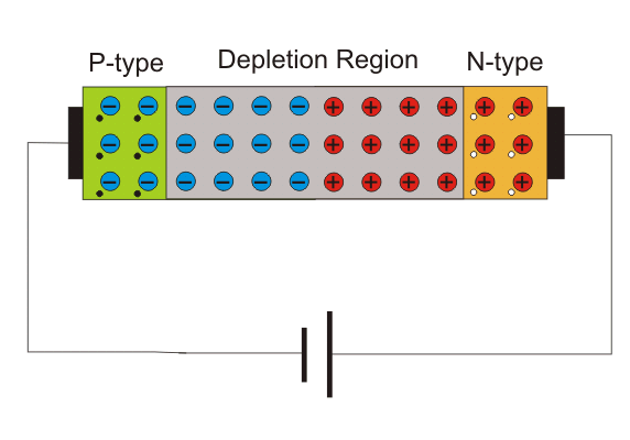
N - side will have a significant number of electrons, and very few holes (due to thermal excitation) whereas the p side will have a high concentration of holes and very few electrons. Due to this, a process called diffusion takes place. In this process free electrons from n side will diffuse (spread) into the p side and recombine with holes present there, leaving positive immobile (not moveable) ions in n side and creating negative immobile ions in p side of the diode. Hence, there will be uncovered positive donor ions in n - type side near the junction edge. Similarly, there will be uncovered negative acceptor ions in p - type side near the junction edge. Due to this, numbers of positive ions and negative ions will accumulate on n - side and p - side respectively. This region so formed is called as depletion region due to the “depletion” of free carriers in the region. Due to the presence of these positive and negative ions a static electric field called as "barrier potential" is created across the p n junction of the diode. It is called as "barrier potential" because it acts as a barrier and opposes the further migration of holes and electrons across the junction.Forward Biased Diode
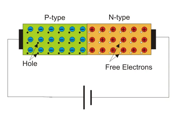
In a PN junction diode when the forward voltage is applied i.e. positive terminal of a source is connected to the p-type side, and the negative terminal of the source is connected to the n-type side, the diode is said to be in forward biased condition. We know that there is a barrier potential across the junction. This barrier potential is directed in the opposite of the forward applied voltage. So a diode can only allow current to flow in the forward direction when forward applied voltage is more than barrier potential of the junction. This voltage is called forward biased voltage. For silicon diode, it is 0.7 volts. For germanium diode, it is 0.3 volts. When forward applied voltage is more than this forward biased voltage, there will be forward current in the diode, and the diode will become short circuited. Hence, there will be no more voltage drop across the diode beyond this forward biased voltage, and forward current is only limited by the external resistance connected in series with the diode. Thus, if forward applied voltage increases from zero, the diode will start conducting only after this voltage reaches just above the barrier potential or forward biased voltage of the junction. The time, taken by this input voltage to reach that value or in other words, the time, taken by this input voltage to overcome the forward biased voltage is called recovery time.Reverse Biased Diode
Now if the diode is reverse biased i.e. positive terminal of the source is connected to the n-type end, and the negative terminal of the source is connected to the p-type end of the diode, there will be no current through the diode except reverse saturation current. This is because at the reverse biased condition the depilation layer of the junction becomes wider with increasing reverse biased voltage. Although there is a tiny current flowing from n-type end to p-type end in the diode due to minority carriers. This tiny current is called reverse saturation current. Minority carriers are mainly thermally generated electrons and holes in p-type semiconductor and n-type semiconductor respectively. Now if reverse applied voltage across the diode is continually increased, then after certain applied voltage the depletion layer will destroy which will cause a huge reverse current to flow through the diode. If this current is not externally limited and it reaches beyond the safe value, the diode may be permanently destroyed. This is because, as the magnitude of the reverse voltage increases, the kinetic energy of the minority charge carriers also increase. These fast moving electrons collide with the other atoms in the device to knock-off some more electrons from them. The electrons so released further release much more electrons from the atoms by breaking the covalent bonds. This process is termed as carrier multiplication and leads to a considerable increase in the flow of current through the p-n junction. The associated phenomenon is called Avalanche Breakdown.Types of Diode
The types of diode are as follow-- Zener diode
- P-N junction diode
- Tunnel diode
- Varactor diode
- Schottky diode
- Photo diode
- PIN diode
- Laser diode
- Avalanche diode
Diode Characteristics
Forward Biasing Characteristic of Diode
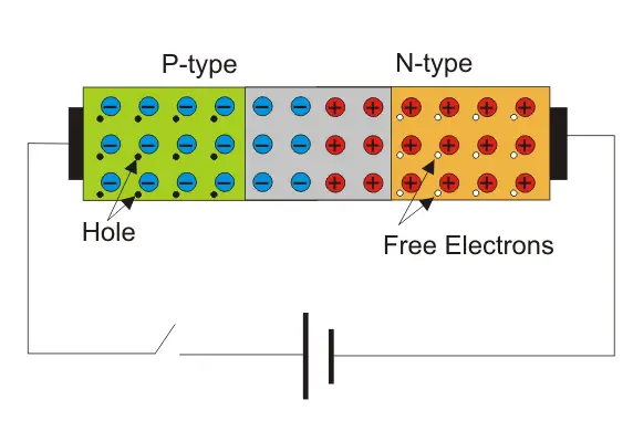
When, P terminal is more positive as compared to N terminal i.e. P- terminal connected to positive terminal of battery and N-terminal connected to negative terminal of battery, it is said to be forward biased.Positive terminal of the battery repels majority carriers, holes, in P-region and negative terminal repels electrons in the N-region and push them towards the junction. This result in increase in concentration of charge carriers near junction, recombination takes place and width of depletion region decreases. As forward bias voltage is raised depletion region continues to reduce in width, and more and more carriers recombine. This results in exponential rise of current.Reverse Biasing Characteristic of Diode
In reverse biasing P- terminal is connected to negative terminal of the battery and N- terminal to positive terminal of battery. Thus applied voltage makes N-side more positive than P-side.Negative terminal of the battery attracts majority carriers, holes, in P-region and positive terminal attracts electrons in the N-region and pull them away from the junction. This result in decrease in concentration of charge carriers near junction and width of depletion region increases. A small amount of current flow due to minority carriers, called as reverse bias current or leakage current. As reverse bias voltage is raised depletion region continues to increase in width and no current flows. It can be concluded that diode acts only when forward biased. Operation of diode can be summarized in form of I-V diode characteristicsgraph. For reverse bias diode, V<0, ID = IS Where, V = supply voltage ID = diode current IS= reverse saturation current For forward bias, V > 0, ID = IS(eV/NVT - 1)
Where, VT = volt’s equivalent of temperature = KT/Q = T/11600 Q = electronic charge = 1.632 X 10 - 19 C K = Boltzmann’s constant = 1.38 X 10 - 23 N = 1, for Ge = 2, for Si As reverse bias voltage is further raised, depletion region width increases and a point comes when junction breaks down. This results in large flow of current. Breakdown is the knee ofdiode characteristics curve. Junction breakdown takes place due to two phenomena:
As reverse bias voltage is further raised, depletion region width increases and a point comes when junction breaks down. This results in large flow of current. Breakdown is the knee ofdiode characteristics curve. Junction breakdown takes place due to two phenomena:
No comments:
Post a Comment